
IBM has unveiled the world’s first sub-1 nanometer chip technology, a breakthrough that could significantly increase AI and cloud computing performance while reducing energy consumption.
Breakthrough “Nanostack” Architecture
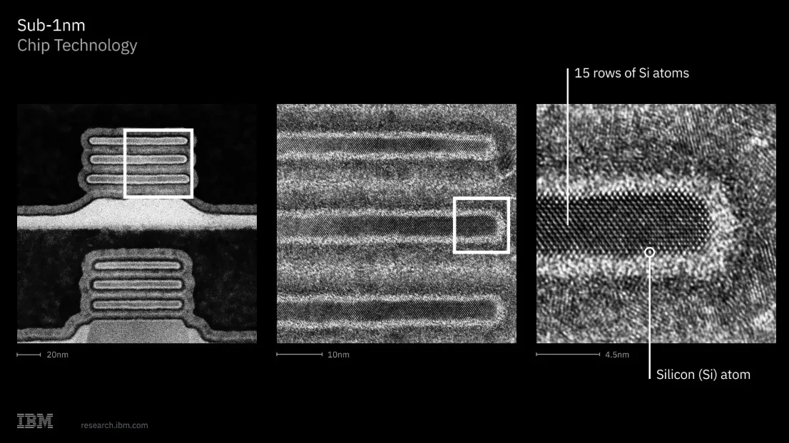
IBM has unveiled the world’s first sub-1 nanometer (nm) chip technology, introducing a new 0.7 nm (7 angstrom) semiconductor architecture designed to deliver significant performance gains while reducing energy consumption. The breakthrough represents a major milestone for the technology industry as demand for AI, cloud computing and advanced digital infrastructure continues to accelerate.
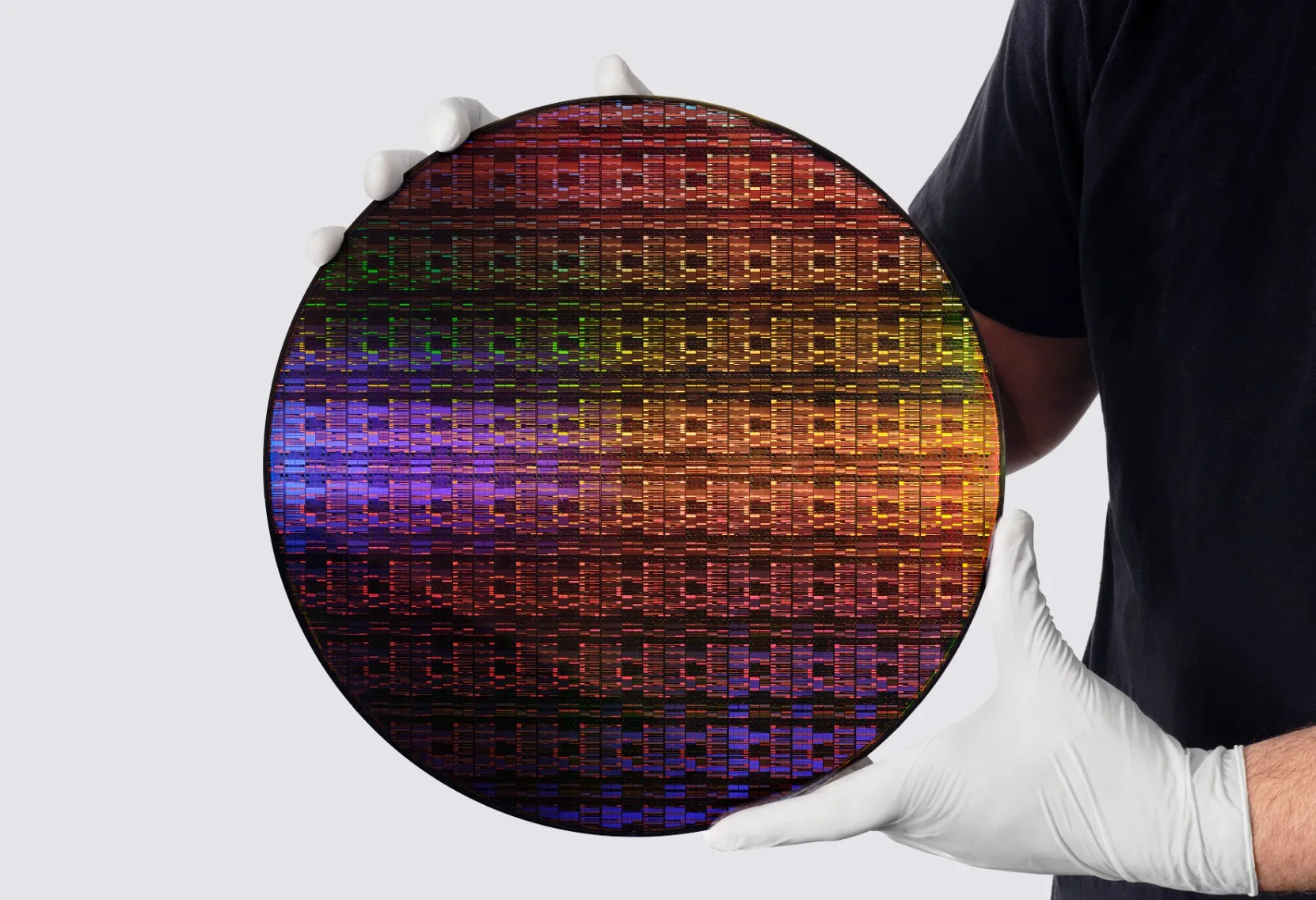
Developed by IBM Research, the new chip incorporates nearly 100 billion transistors on a chip the size of a fingernail—almost double the density of IBM’s 2 nm chip announced in 2021. At its core is a revolutionary three-dimensional “nanostack” transistor architecture that reimagines how chips are built, extending semiconductor scaling beyond the limits of traditional designs.
Driving More Sustainable AI Infrastructure
As organisations deploy increasingly complex AI workloads, improving compute efficiency has become a critical sustainability challenge. IBM projects the new sub-1 nm technology could deliver up to 50% higher performance or 70% greater energy efficiency compared with its 2 nm generation, enabling more powerful computing while reducing the energy required to support data-intensive applications.
The breakthrough highlights how semiconductor innovation can help address one of the technology sector’s fastest-growing environmental challenges: the rising energy demand associated with AI, cloud infrastructure and high-performance computing.
“IBM’s latest chip breakthrough marks a landmark moment in computing, pushing technology beyond the nanometer era to the scale of atoms. With our new nanostack architecture, we’re not just making smaller transistors, we’re reinventing how chips are built to deliver dramatically more power and energy efficiency,” said Jay Gambetta, Director of IBM Research and IBM Fellow.
“This industry-first innovation continues IBM’s legacy of leading in next-generation technologies and sets the foundation for the next era of computing.”
Reinventing Semiconductor Design for the Next Decade
The new nanostack architecture represents a significant evolution in chip design. Unlike conventional transistor structures, nanostack vertically stacks and staggers nanosheet transistors, enabling greater transistor density while optimising performance and power efficiency across different layers of the chip.
IBM researchers also demonstrated that the architecture can significantly improve memory scaling, helping support the growing data and bandwidth requirements of advanced AI systems.
The company believes the innovation provides a roadmap for continued semiconductor scaling over the next decade, even as the industry approaches atomic-level manufacturing limits.
Supporting Long-Term Technology and Climate Goals
The development underscores the increasingly important link between semiconductor innovation and sustainability objectives. More efficient chips can help reduce the energy footprint of AI, cloud services, enterprise computing and critical digital infrastructure, supporting efforts to lower emissions while meeting growing demand for computing capacity.
The technology was developed at IBM’s semiconductor research facility in Albany, New York, where the company is collaborating with industry partners on next-generation manufacturing technologies, including High Numerical Aperture Extreme Ultraviolet (High NA EUV) lithography.
With commercial adoption potentially beginning within the next five years, IBM’s sub-1 nm breakthrough demonstrates how advances in chip design can help deliver both higher performance and greater energy efficiency—critical requirements for the future of AI-driven, sustainable digital infrastructure.
This article was produced by the editorial team at North America Outlook and published as part of the Outlook Publishing global network of B2B industry magazines.
Outlook Publishing delivers industry insights, company stories, and sector coverage across manufacturing, mining, construction, healthcare, supply chains, food production, and sustainability.
North America Outlook provides ongoing coverage of organisations and developments shaping industries across North America.